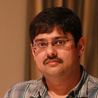
Presented by Dr. Souvik Mahapatra
Melchor Visiting Professor in Engineering
Professor of Electrical Engineering, Indian Institute of Technology, Bombay
Modern logic and memory FETs consist of a dual (or triple) layer gate insulator stack. Charging of defects (pre-existing and generated during operation) in the gate stack shifts the performance of the FETs and is responsible for the eventual reliability of these devices and associated systems. In this talk, we will discuss several mechanisms and models that have been proposed in the literature to model the time kinetics of these defects, and benchmark those against experimental data. Examples will be shown using Bias Temperature Instability in logic FETs, and modifications (if any) needed to apply these models for memory devices will be discussed.

Souvik Mahapatra received his PhD from IIT Bombay in 1999. During 2000-01, he was with Bell Laboratories, Murray Hill, NJ. Since 2002, he has been with the Department of Electrical Engineering at IIT Bombay and is presently a full professor. His current research interests are CMOS device scaling and reliability, and device-circuit co-design for co-optimisation of power, performance, and reliability. He has published more than 150 papers in peer reviewed journals and international conferences, delivered invited talks at major international conferences, including IEEE IEDM and IRPS, and has been actively collaborating with several global semiconductor industries. He is a fellow of IEEE (for contributions to CMOS transistor gate stack reliability), a fellow of INAE, and a distinguished lecturer of the IEEE Electron Devices Society.
Host: Prof. Suman Datta sdatta@nd.edu
Co-sponsored by the College of Engineering.
Originally published at nano.nd.edu.